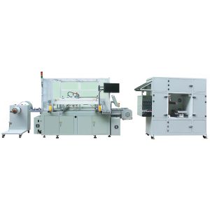
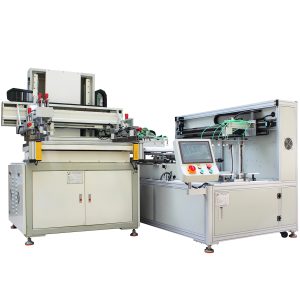
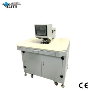
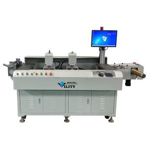
PCB Fully Automatic Screen Printing Line
Printed Circuit Board (PCB) Fully Automatic Screen Printing Line
Screen Printing Press for Circuit Boards/PCB Board Flatbed Silkscreen Printer/Automatic Pcb Printing Machinery/PCB Screen Printing Equipment
Printed circuit board screen printing
Printed circuit board (PCB)
Screen printing methodology can be applied to print graphic, marks, conductive ink and isolated ink directly onto foil or panel. Our production process is complied with international standard procedure for quality control to produce high precision screen printer, which can be applied to print fine line (circuits, legend and marks) and wet film process plug-via as well as solder mask.
What is the Silkscreen in a PCB?
Silkscreen is a layer of text or graphics printed on the PCB’s surface that provides information about the components, their placement, and other relevant details. This layer is typically printed in white or black ink and is placed on top of the copper traces and other layers that make up the PCB.
The silkscreen layer on a PCB is not electrically conductive, which means that it does not affect the electrical performance of the circuit. Instead, it is used as a guide for the person assembling or servicing the PCB. They are typically made up of a layer of ink that is applied to the surface of the board.
The ink used for silk screening on PCBs is usually a high-contrast color, such as white or black, which provides clear and easy-to-read markings. It is typically a specialized ink that is resistant to the harsh chemicals and high temperatures used during the PCB manufacturing process. This ensures that the silk screen markings remain intact and legible throughout the entire PCB manufacturing process, including cleaning, etching, and soldering.
A PCB (Printed Circuit Board) is used to connect and control electronic components in various devices such as computers, smartphones, and televisions. PCB fabrication is an extensive process that requires multiple component steps to achieve the desired result.
In a standard PCB production process, the manufacturers decide on a non-conductive substrate that forms the base of the PCB, followed by a coating layer of copper, which is then laminated with a fine film that has PCB circuits designed and printed on it. After the PCB is passed through UV light, only the copper portions visible to the UV rays are permanent. This PCB sheet is then dipped into an etching solution, removing all the excess copper and creating the desired circuit on it. This is followed by multiple processes like applying a solder mask, surface finish, and finally, a Silkscreen.
 Screen printing machine


